Fast, Fast, Fast
Conventional assembly automation techniques cannot provide the continuous improvement in cost and yield necessary for today’s environment. PI’s groundbreaking parallel gradient search allows simultaneous optimization of multiple degrees of freedom, elements and channels. To date, these alignments needed to be performed in serial fashion in time-consuming loops, since dependencies are unavoidable between degrees of freedom and between elements. For example, alignment of an element in theta-X/theta-Y usually must be interrupted to correct for geometric errors introduced in X and Y, and then the process repeated. With PI’s parallel technology, these alignments can typically be performed in one step, reducing the time required by typically 99% or more while improving yield. Similarly, dependencies between elements formerly necessitated gradual, sequential alignments of each in a loop to achieve an overall consensus alignment. Parallel optimization allows these alignments to be achieved in one step.
That’s All You Need for Active Alignment
The very heart of PI´s Active Alignment system is the >> F-712.HU1 Fast Multi-Channel Photonics alignment system, which includes the E-712 motion controller. The gradient search algorithm is built into the firmware of the controller. When optical power is the figure-of-merit to be optimized, the >> F-712.PM1 Power Meter is of help. Other figures of merit are generally straightforward to accommodate, such as MTF, extinction ratio, modal quality, and other metrics.
PI’s Unique Parallel Gradient Search Technology
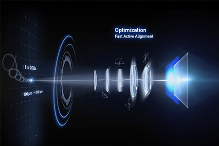
Based on micron- or even nanometer-scale exploratory motions of the alignment system, the algorithm measures the local gradient of a figure-of-merit such as image quality of a camera lens system or the output power of a laser. This gradient is then automatically followed until the desired position and orientation of the elements is reached. The routine allows excellent tracking and therefore it is possible to compensate any drift effects. PI’s unique approach allows multiple gradient search routines to proceed in parallel. This means optimization of multiple elements, degrees-of-freedom, channels, etc., can proceed simultaneously. This breakthrough capability can reduce overall optimization times by two or more orders of magnitude.

Simultaneous Adjustment of Several Single Elements
The true power of this new class of positioning however only unfolds, when it comes to the parallel or simultaneous adjustment of several single elements in one go. Instead of time-consuming optimization of one element after the other in lenghty loops, interleaved with metrology and other processes, the gradient search algorithm allows for simultaneous or parallel alignment of several elements in one go.
This results in a drastic reduction of process-times, previous applications achieve 99% or more reduction of throughput time.

PI – Automated Multichannel Fiber Array Alignment
Connecting optical fibers (single-mode or multi-mode fibers) to silicon photonic devices (SiP) is still one of the most challenging and intricate tasks in test and packaging of these devices.
Based on its unique “Fast Multi-Channel Photonics Alignment” systems PI has successfully developed an automated subsystem for waferprobing with high throughput. The video now presents approaches for automation of test and packaging at chip level.

Numerous Applications for Active Alignment
In more and more photonic and optical systems, the exact geometric positioning of individual elements plays a crucial role in the overall functionality. Active Alignment offers unique optimization possibilities for this:
- The use in the quality assurance of silicon photonics has already been established since 2015-2016 with the first high-throughput photonic wafer probers, volume manufacturing, and assembly tools. For both, wafer probing and chip testing, it is important to check the functionality of active and passive optical structures on the chip (i.e., waveguides, light and photo diodes) before packaging. For this purpose, glass fibers are precisely positioned to the corresponding chip structures that a quality check can be performed.
- Volume manufacturing of high-bitrate consumer optical cables such as HDMI, USB, and Thunderbolt can greatly benefit from PI’s parallel optimization technology. Not only is the multiple-degree-of-freedom alignment of the cable connectors greatly accelerated by adoption of PI parallel optimization, but both sides of the cable can be assembled simultaneously.
- Smartphone cameras are manufactured by the billions each year and are seeing a blistering pace of innovation, with ever-advancing quality and adoption of higher-ratio optical zoom, scene recognition and focus-detection capabilities. PI’s parallel optimization technology can greatly reduce the time required to assemble these complex mechanisms to relentlessly finer tolerances.
- In volume laser manufacturing, complex cavity designs incorporate multiple refractive, reflective and diffractive elements which all must be mutually optimized in order to meet power output and modal quality specifications. PI’s parallel alignment technology can greatly reduce the time required to achieve this while allowing real-time compensation of drift during manufacturing operations.
- Numerous other applications in technical optics (e.g., LIDAR systems), life sciences, quantum computing, or data storage can benefit from active alignment technology.