The entire chip manufacturing process consists of 400 to 800 production steps. At all critical points in the manufacturing process, inspection processes are essential to ensure the high quality and reliability of the final products. Additionally, they help secure a defined yield of cost-intensive chip production. Moreover, with each node, the inspection process becomes more challenging and costly. Nowadays, defect tolerance is increasingly low due to process shrinks, smaller features, design complexities, and the integration of heterogeneous components at wafer level. For this reason, and to reduce costs, today’s optical inspection tools must detect defects in the nanometer range, enabling damaged structures to be removed from the process at an early stage.
These tools often work in scanning modes where a specific position must be identified and subsequently approached with high precision, or for applications where it is necessary to follow a trajectory for processing steps. Within our product portfolio, PI provides the integrated solution to support both substrate carriers and objective assembly.
Key Features of the Motion Solution
- Defect and edge placement error (EPE) inspections
- Highly adaptive surface inspection
- High throughput
- Reduced dynamic errors and optimized focusing time
- High reliability at high duty cycles
- Reduced cost of ownership
- Secured yield
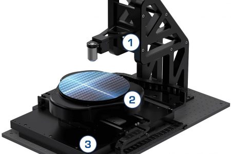
1. Z Axis – High-Dynamic Laser Focus Control
- Wear-free, lever-amplified piezo drives for 24/7 operations without particle generation
- Mechanical design with high stiffness and high resonant frequencies provide high dynamics and short settling times and allows high payload of larger objectives
- Up to 800 μm travel range
- Fine positioning with subnanometer resolution
>> P-725 PIFOC® Objective Scanner
2. θX/θY/Z Axis – High-Precision Wafer Alignment and Positioning
- Parallel-kinematic design for wafer adjustment and offset corrections in three dimensions
- Direct drive linear motor with air bearings for high-precision levelling
- Frictionless design with minimal hysteresis provides high repeatability and adjustments in the nanometer range
- Low-profile design for easy integration
- Maintenance-free with long lifetime in 24/7 operations
>> A-523 Z Tip/Tilt Stage
3. XY Axis – Wafer Step-and-Scan Motion
- Air-bearing planar scanner with ironless linear motors for high, cog-free scanning speed and fast stepping and settling times
- Contact and wear-free design allows 24/7 high duty cycle operations with minimal runout errors and nanometer straightness and flatness
- High-resolution absolute linear encoder option for fast startup, reliability, and safety
- Low profile, monolithic design allows easy integration to system level solutions for compact installation space
- Wide carriage insures increased stiffness
>> A-311 Air Bearing Planar Scanner
4. Advanced Automation Control
- EtherCAT® motion control and drive modules provide open network connectivity
>> Controller & Drives - Advanced algorithms provide fast step-and-settling, high in-position stability, and exceptional constant scanning velocity
>> ServoBoost™ - Fast digital interchange to trigger fast focus on Z axes
Original article published: https://www.physikinstrumente.com/en/knowledge-center/products-and-systems-applications/wafer-inspection-and-metrology/?utm_medium=social&utm_source=linkedin.com&utm_campaign=IA&utm_content=Wafer-Inspection-and-Metrology